

ASPS 2026 Visit Report: Next-Generation Semiconductor Packaging Opening with Glass Substrates, HBM, and Optical Interconnects
Core Summary
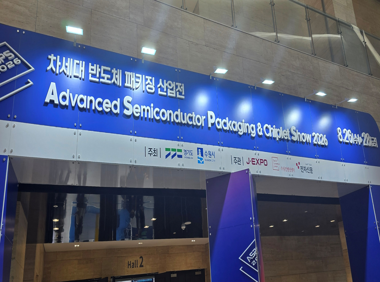
- Event Overview: The 2026 Next-Generation Semiconductor Packaging Industry Exhibition (ASPS), held at the Suwon Convention Center from August 26 to 28, was an event to confirm the cutting edge of AI/HPC semiconductor packaging technology.
- Key Topics: Glass Interposer, HBM heat management, and Optical Interconnect (CPO) technology were the main focal points to resolve data transfer bottlenecks between chips.
- Common Flow: Participating companies were moving towards securing mass production and cost efficiency beyond technical completion.
Main Contents
The keyword that ran through this exhibition was ‘Interconnect.’ How quickly and efficiently data transfer occurs between chips and systems is becoming a core factor in AI semiconductor competitiveness.
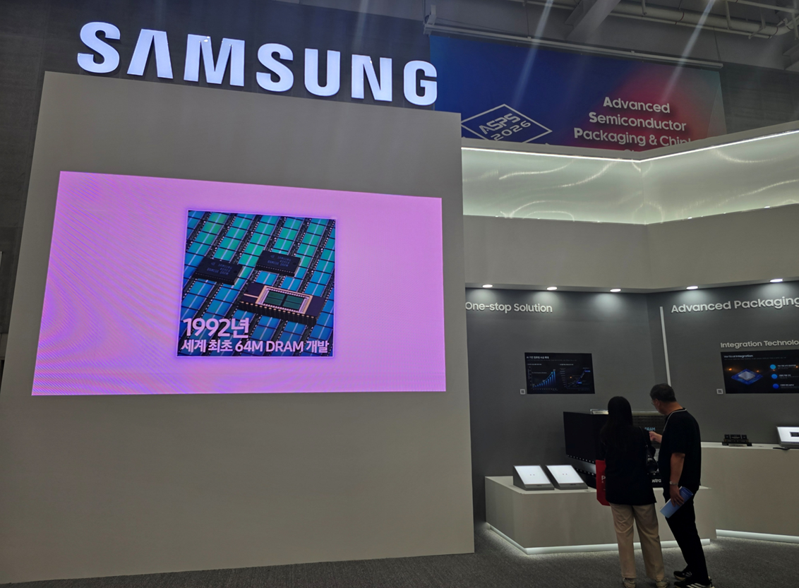
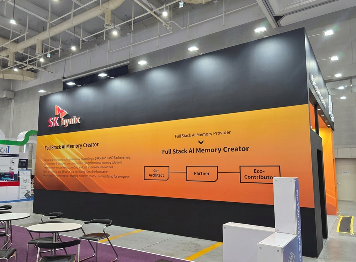
Samsung Electronics and SK Hynix, leading in the memory semiconductor market, showcased different core technologies. Samsung focused on next-generation packaging and Co-Packaged Optics, while SK Hynix emphasized HBM heat management technology.
This visit report summarizes the direction of the next-generation packaging industry shown by ASPS 2026, focusing on key exhibitor contents.
1. Why is this exhibition, ASPS 2026, attracting attention?
As AI and HPC industries expand, the volume of data transfer between chips has surged, and traditional electrical signal methods have faced limitations in bandwidth, power, and distance. ASPS 2026 was a place where core technologies like Glass Interposer, HBM heat management, and Optical Interconnects gathered to solve these bottlenecks.
| Category | Samsung Electronics | SK Hynix |
| Core Exhibition Fields | 2.3D, 3D Packaging / CPO1) | HBM / Heat Management |
| Key Technologies | 2.3D Cube-E, 3D Cube-T/H | iHBM (ICE2)) |
| Core Materials/Structures | Si-Bridge, Photonic IC | Core/Base Die, TSV |
| Process Efficiency | Shortening of inter-chip connection distance | Optimization of heat dissipation paths |
| Investment and cost improvement | Enhancement of system design efficiency | Reduction of thermal resistance by over 30% |
| Goals | CPO(Co-Packaged Optics) | Full Stack AI Memory |
2) ICE (Integrated Cooling Element): Silicon material that does not conduct electricity but has high thermal conductivity.
2. Three core highlights of ASPS 2026:
① Ultra-fine packaging technologies such as Chiplet and hybrid bonding
: You can confirm the chiplet structure that connects multiple chips into one to maximize semiconductor performance.
: Major companies including Samsung Electronics and SK Hynix showcase how they implement packaging solutions in real life.
② Next-generation game changer, “Semiconductor Glass Substrate”
: You can see materials and equipment technology related to glass substrates that are advantageous for microcircuit implementation, low heat generation, and large-area application.
: It is possible to see the commercialization stage and ecosystem development of glass substrate processing equipment and TGV technology presented by domestic and international component companies.
③ Thermal management for high-performance AI semiconductors and related materials/parts
: As AI chip development progresses, heat control has emerged as a key performance factor, increasing the importance of high-efficiency heat dissipation materials.
: It is possible to verify the current level of advanced packaging materials and post-processing ecosystem supporting technology for withstanding ultra-high heat environments.
3. AI Memory Game Changer: Samsung’s Hyper-connection and SK Hynix’s Ultra Thermal Management
■ Samsung Electronics: Opening the Hyper-connection Era with 3D Integration and CPO
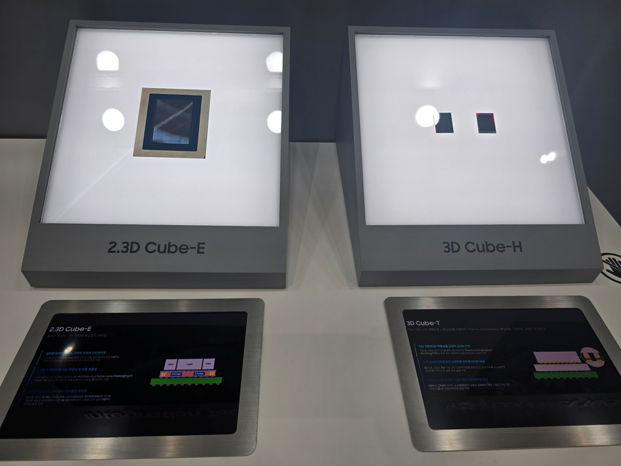
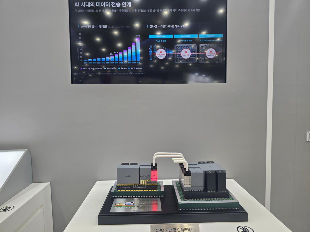
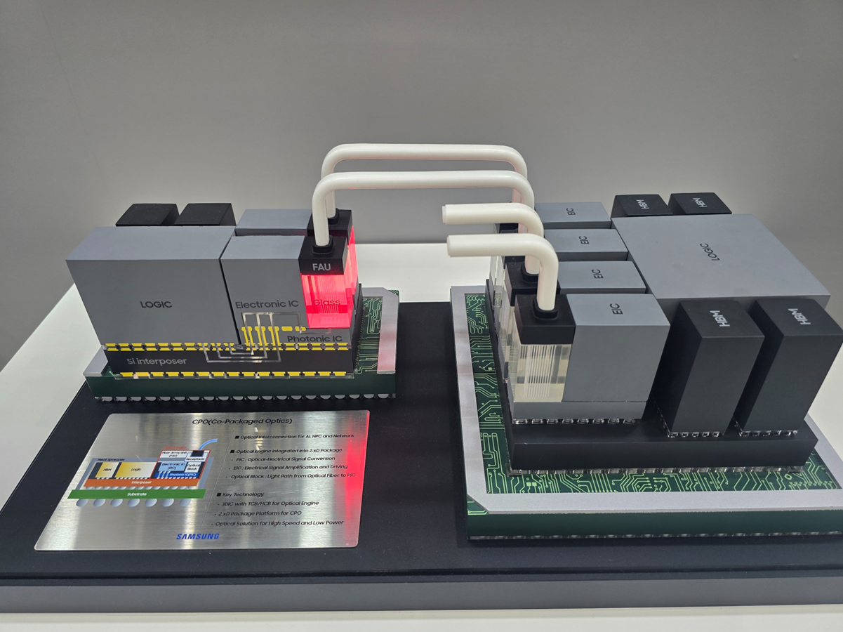
Samsung Electronics showcased heterogeneous bonding packaging and optical interconnect technology to address data transmission limits in the AI era.
The entire process, from memory manufacturing to foundry and advanced packaging, was unified under the theme of ‘One-Stop Solution’, demonstrating a comprehensive semiconductor company’s capabilities.
① Heterogeneous Integration Packaging
: Shorten the connection distances between chips by vertically and horizontally integrating Top Die, Bottom Die, and HBM using Si-Bridge and ISC, thereby enhancing bandwidth and reducing latency.
①-1. 2.3D Cube-E enables the horizontal integration of silicon-embedded structures like CPU, GPU, and HBM Die.
①-2. 3D Cube-T, TSV-based Vertical Stacking
: Supports high-density 3D IC applications such as HBM and CMOS image sensors (CIS) by applying u-Bump and Thermo Compression Bonding (TCB).
①-3. 3D Cube-H, Bump-less Hybrid Cu Bonding
: Connect TSV-based logic dies directly with hybrid Cu bonding to achieve the highest level of integration and the shortest vertical signal paths.
② CPO (Co-Packaged Optics), Optical Interconnects
: Integrate Logic·Electronic IC (for computation) and Photonic IC (optical circuit chip) on top of Si Interposer, and connect optical signals directly via Fiber Array Unit to realize high-speed, low-power data transfer.
Samsung Electronics is proposing solutions for next-generation AI infrastructure by integrating chips from different processes into one system using heterogeneous integration technology.
■ SK Hynix: iHBM Solution for Managing HBM Heat
In the AI accelerator era, the more stacks of HBM piled up, the greater the heat dissipation problem. SK Hynix has presented a structural solution that effectively releases this heat.
The core is to insert ICE (Integrated Cooling Element) between the core and base die to optimize the heat flow path.
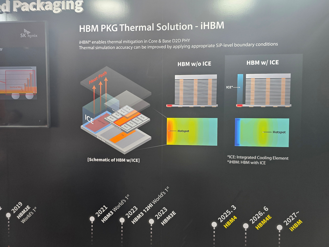
iHBM Thermal Management Solution
Structure: Core & Base Die D2D PHY
- Goal: To alleviate localized heat concentration (Hotspot) at the junction of core and base die.
- Method: Place ICE (Integrated Cooling Element) vertically along the heat-generating path to quickly disperse heat upward.
- Effect: Compared to before applying ICE, the Hotspot temperature distribution has significantly improved, and the accuracy of SiP-level thermal simulation has also been enhanced.
HBM Roadmap
- 2019 HBM2E (world’s first) → 2021 HBM3 (world’s first) → 2023 HBM3 12Hi / HBM3E
- 2025.3 HBM4 → 2026.6 HBM4E → 2027~ Expansion of iHBM application
- SK Hynix aims to serve as a ‘Full Stack AI Memory Creator’ by acting as Co-Architect, Partner, and Eco-Contributor.
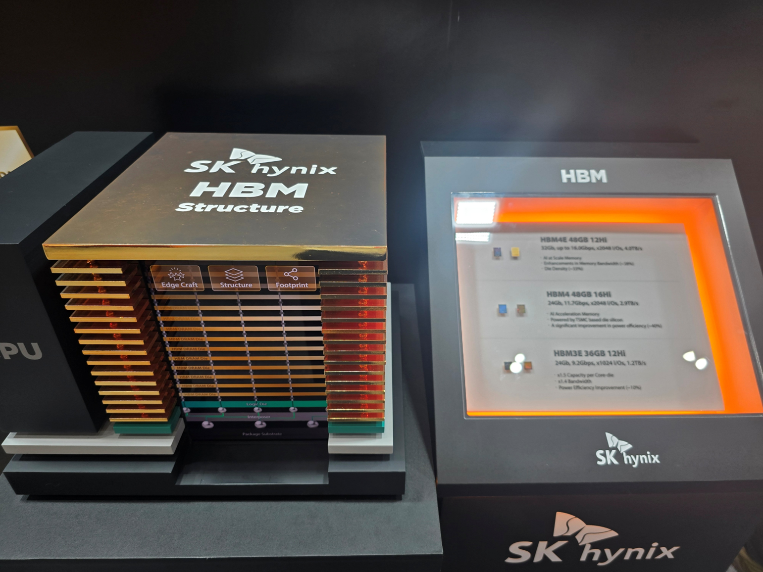
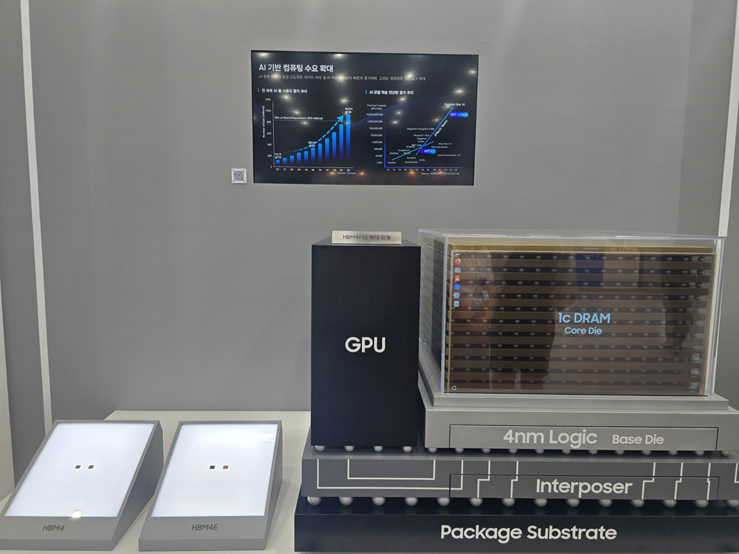
What the HBM4/4E expansion models show
① We were able to confirm a structure in which the interposer and core die (1c DRAM) were precisely stacked on a 4nm logic base die.
② HBM4 targets AI-scale memory with x2048 I/O, while HBM4E offers up to 16.0 Gbps bandwidth.
③The entire stack structure, including the package substrate that connects to the GPU, was displayed as a physical model.
Improving HBM’s bandwidth and power efficiency is a key factor in expanding AI infrastructure.
4. Visitor Feedback
This ASPS 2026 site was, in one word, a ‘total firefight of technologies to break the limits of AI/HPC semiconductors.’
Especially, Samsung Electronics and SK Hynix, the two giants of memory, presented physical models and concrete roadmaps, demonstrating Korea’s overwhelming technological prowess in semiconductors.
The fierce competition for dominance made this very clear.
Ultimately, the next battlefield for AI semiconductors is undoubtedly ‘Advanced Packaging’. Companies that overcome miniaturization limits and achieve mass production efficiency will lead the future AI market.
They will take the lead.
Through this visit, I was able to clearly identify the future roadmap that Korea’s semiconductor industry will carve out amid this immense trend.